|
EMI Automation Scanning System
|
|
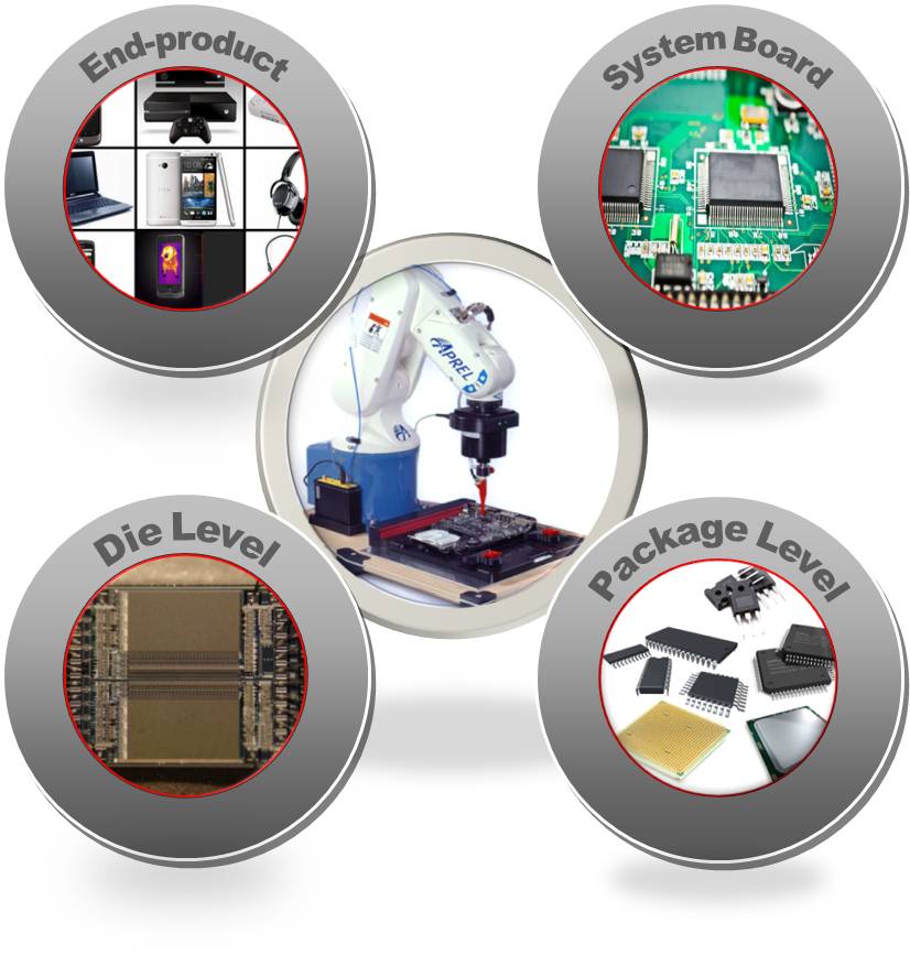
- The Near Field Electromagnetic measurement system is an advance system with robot controlled that is fully support development and design activities for PCB, Integrated Circuit, Mobile Telephone, Notebook PC and Antenna.
- In traditional applications, the system of EMI scanning can solve EMI problems for international standards; in advanced applications, we provide the EM crosstalk, shielding capability for PCB layout and material verifications.
|
|
EMI Shielding Material Analysis
|
|
|
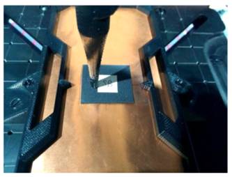
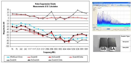
- Integrated circuits or Device PCB can have resonances or radio frequency content that may impact a design and certificate.
- The composites material used to contain the integrated circuit or package can reduce the magnitude of these resonances.
- Considerations can be made to the design of the packaging materials and EMI absorber to reduce emissions.
|
|
Electrostatic Discharge (ESD) Analysis
|
|
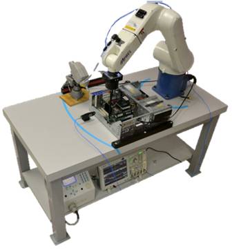
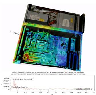
- EM-ISight-ESD system is controlled by APREL software, controlling the robot position and ESD source generator.
- The magnetic H-Field probes employ an advanced design, these highly shielded magnetic probes set the industry standard for electric field rejection capturing ESD events in line with IEC-61000-4 standard for conducted and air discharge modes.
- Through developing the measurement methodologies needed to capture an ESD event in a spatial location the time and frequency can be resolved through the integration of a Real-Time Spectrum Analyzer and Oscilloscope.
|